MIPI M-PHY Introduction
The MIPI M-PHY (Mobile Industry Processor Interface M-PHY) is a high-speed serial communication physical layer specification developed by the MIPI Alliance. It serves as the foundational layer for various high-bandwidth mobile and embedded protocols, most notably UFS (Universal Flash Storage).
Why M-PHY Exists
As mobile devices evolved, the need for higher storage bandwidth conflicted with the requirement for lower power consumption. Traditional parallel interfaces like eMMC were reaching their limits:
- Pin Count: Parallel interfaces require many pins (8-bit data bus + control signals)
- Power: Multiple simultaneous switching pins consume significant power
- Speed: Parallel interfaces suffer from signal integrity issues at high speeds
- EMI: Parallel buses generate more electromagnetic interference
M-PHY addresses these challenges through high-speed serial communication with sophisticated power management.
Key Design Characteristics
1. Power Efficiency
MIPI M-PHY employs burst operation mode, switching intelligently between states:
- Burst Mode: Transmit data at high speed, then return to low-power mode
- Rapid State Transitions: Fast sleep-to-active transitions (microseconds)
- Granular Power States: Multiple power modes for different scenarios
This approach is crucial for mobile devices where battery life is paramount. During idle periods, M-PHY can drop to near-zero power consumption.
2. High Data Rates
M-PHY supports impressive bandwidth scaling:
- M-PHY v1.0: Up to 1.46 Gb/s per lane
- M-PHY v2.0: Up to 2.9 Gb/s per lane
- M-PHY v3.0: Up to 5.8 Gb/s per lane
- M-PHY v4.0: Up to 11.6 Gb/s per lane
- M-PHY v5.0: Up to 23.2 Gb/s per lane
For perspective, UFS 4.0 storage with dual-lane M-PHY v5.0 can achieve 46.4 Gb/s (5.8 GB/s) - far exceeding SATA SSDs.
3. Low Pin Count
M-PHY achieves high bandwidth with minimal pins:
- Single Lane: Just 2 differential pairs (TX and RX)
- Dual Lane: 4 differential pairs total
- Scalable: Can add lanes as needed (1-8 lanes typical)
This is critical for mobile SoCs where every pin counts.
4. Lane Scalability
M-PHY allows dynamic lane configuration:
- UFS Storage: Typically 1 or 2 lanes
- Camera Interfaces: May use multiple lanes for high-resolution sensors
- Display Links: CSI (Camera Serial Interface) uses M-PHY for high-speed video
The protocol can adapt bandwidth by activating/deactivating lanes based on workload.
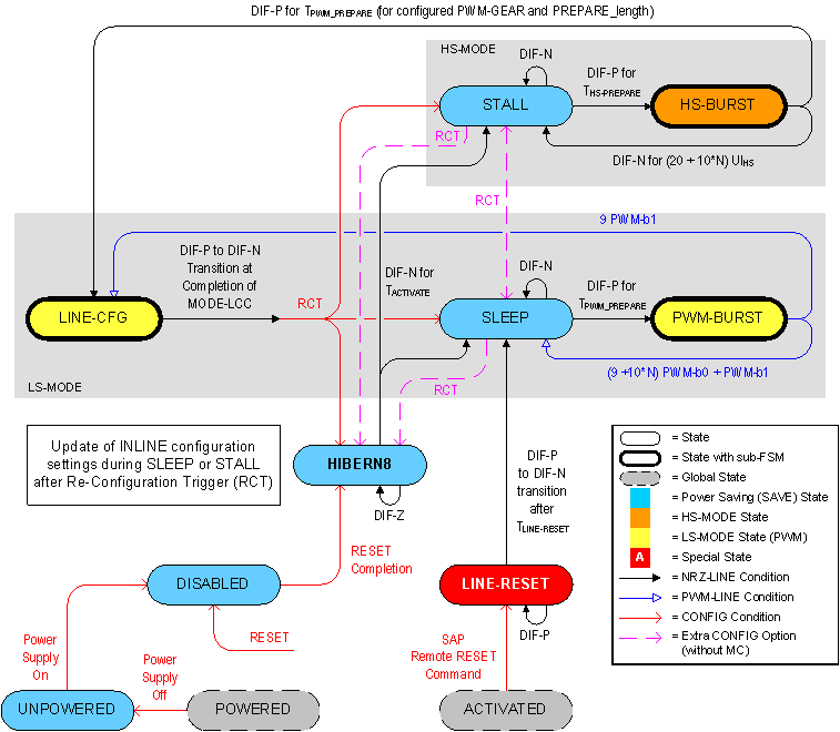
M-PHY Line States
Understanding M-PHY requires knowing its four fundamental line states:
DIF-P (Differential Positive)
A positive differential voltage actively driven by the transmitter. This represents a logical ‘1’ in the data stream. The TX side drives the positive line high and negative line low, creating a positive voltage differential.
DIF-N (Differential Negative)
A negative differential voltage driven by the transmitter. This represents a logical ‘0’. The polarity is opposite to DIF-P, with the positive line low and negative line high.
DIF-Z (Differential Zero)
A zero differential voltage maintained by the receiver (RX) when the transmitter is not driving. The receiver pulls both lines to approximately the same voltage, creating no differential. This state is used during idle periods and certain handshaking sequences.
DIF-Q (Differential Quiet)
An unknown or floating voltage where neither TX nor RX is driving the line. This represents a high-impedance state. DIF-Q is typically used during power state transitions or error conditions.
These states enable M-PHY to communicate not just data, but also control information through line state sequences.
M-PHY Power States
M-PHY defines a sophisticated power state machine:
High-Speed (HS) Modes
HS-G1 through HS-G5: Active data transmission at progressively higher speeds
- HS-G1: 1.46 Gb/s per lane
- HS-G2: 2.9 Gb/s per lane
- HS-G3: 5.8 Gb/s per lane
- HS-G4: 11.6 Gb/s per lane
- HS-G5: 23.2 Gb/s per lane
PWM (Pulse Width Modulation) Modes: Lower speed, lower power option for non-critical data
- PWM-G1 through PWM-G7: 3.6 Mb/s to 15.1 Mb/s per lane
Low-Power States
STALL: Brief pause during transmission (microseconds)
SLEEP: Deep sleep state requiring wakeup sequence (milliseconds)
HIBERN8: Deepest sleep state, saves maximum power but requires longer wakeup
LINE-RESET: Reset sequence to recover from errors
State Transitions
     [HIBERN8]
         ↓ (wakeup)
      [SLEEP]
         ↓ (activate)
      [STALL]
         ↓ (burst)
    [HS-BURST] ←→ [HS-PREPARE]
         ↓ (idle)
      [STALL]
         ↓ (sleep command)
      [SLEEP]
Fast transitions between STALL and HS-BURST enable the efficient burst-mode operation that makes M-PHY power-efficient.
M-PHY in UFS Architecture
In a UFS storage system:
Physical Layer (M-PHY): Handles actual signal transmission
- Serialization/deserialization
- Encoding/decoding (8b10b or 128b132b)
- Power management
Data Link Layer (UniPro): Sits above M-PHY
- Error detection and retry
- Flow control
- Link startup and training
Transport Layer (UFS): Application-level protocol
- SCSI command processing
- Power management commands
- Device configuration
Applications Beyond UFS
M-PHY is the foundation for multiple MIPI protocols:
CSI-3 (Camera Serial Interface): High-resolution camera connectivity
DigRF (Digital RF Interface): Baseband-to-RF chip communication
UniPro: General-purpose protocol for chip-to-chip IPC
LLI (Low Latency Interface): Inter-processor communication in modems
SSIC (SuperSpeed Inter-Chip): USB 3.0 protocol over M-PHY for chip-to-chip links
This versatility makes M-PHY a cornerstone of modern mobile SoC design.
Signal Integrity and Design Challenges
Achieving 23.2 Gb/s requires careful PCB design:
Differential Pair Routing: Impedance-controlled differential pairs (typically 100Ω)
Length Matching: TX+/TX- pairs must match within 0.1mm; lane-to-lane within 5mm
Via Design: Minimize vias; use back-drilling to remove stubs
Noise Isolation: Guard traces or ground planes between lanes
Power Supply: Clean power rails with appropriate decoupling
Poor signal integrity leads to increased bit error rates (BER), forcing M-PHY to lower its gear (speed grade) or even fail to train.
Power Management Example
Consider a smartphone reading a 100MB photo album:
- HIBERN8: UFS idle, ~0mW
- Wakeup: M-PHY exits HIBERN8 (~100μs)
- HS-G4 Burst: Transfer 100MB at 11.6 Gb/s (~70ms at 1.45 GB/s effective)
- Stall: Brief idle
- SLEEP: Return to low power after command completion (~1ms transition)
Total active time: ~171ms. The burst approach minimizes power compared to staying active continuously.
Comparison with Other Interfaces
| Interface | Bandwidth | Lanes | Power | Use Case |
|---|---|---|---|---|
| eMMC | 400 MB/s | 8-bit | Medium | Legacy mobile storage |
| UFS 2.1 | 1.45 GB/s | 2-lane M-PHY | Low | Mid-range phones |
| UFS 3.1 | 2.9 GB/s | 2-lane M-PHY | Low | High-end phones |
| UFS 4.0 | 5.8 GB/s | 2-lane M-PHY | Low | Flagship phones |
| SATA | 600 MB/s | 1-lane | Medium | PC storage |
| PCIe 3.0 | ~1 GB/s | 1-lane | Higher | PC NVMe SSDs |
M-PHY’s combination of high bandwidth and low power is unmatched for mobile applications.
Debugging M-PHY Issues
Common problems and diagnosis:
Training Failure: Check signal integrity, PCB layout, component placement
Gear Downgrade: Link trains but at lower speed - indicates marginal signal quality
BER Issues: Bit errors during operation - review power supply noise, EMI sources
Hibernate Failure: Cannot enter/exit low-power states - check power management implementation
Tools: High-speed oscilloscopes, protocol analyzers, BERT (Bit Error Rate Testers)
Future Evolution
M-PHY continues evolving:
M-PHY v6.0: Expected to reach 46.4 Gb/s per lane
PAM-4 Modulation: Multi-level signaling for higher bandwidth density
Advanced Power Management: Even finer-grained power states
Longer Reach: Supporting slightly longer cable connections
Conclusion
MIPI M-PHY represents a masterful balance of competing requirements: high bandwidth, low power, minimal pins, and cost-effectiveness. Its success in mobile storage (UFS) has made it ubiquitous - likely powering the storage in the device you’re reading this on.
For embedded systems engineers, understanding M-PHY is essential when designing systems with UFS storage, CSI cameras, or any high-speed mobile interface. The physical layer may be invisible to software, but it fundamentally determines what’s possible at higher layers.
Whether you’re optimizing smartphone storage performance, designing an automotive infotainment system, or developing the next generation of IoT devices, M-PHY knowledge provides the foundation for making informed architectural decisions.
References
- MIPI Alliance M-PHY Specification v5.0
- MIPI UniPro Specification v2.0
- JEDEC UFS Specification v4.0
- High-Speed Digital Design: A Handbook of Black Magic by Howard Johnson
There are 2 operating modes: HS-MODE and LS-MODE. For each operating mode there are save state. STALL is the save state of HS-MODE. SLEEP is the save state of LS-MODE.
HIBERN8 state is the ultra low power consumption mode which only maintaining the configuration settings.
The detail of the state machine diagram is showing like below : Please note that for every state switching it is together with the line state change. So line state is important signal for the state indication. For example, the state switchs from PWM-BURST to the SLEEP. The line state need change from the DIF-P to DIF-N. The SLEEP state is confirmed after the state is change completely to the DIF-N.